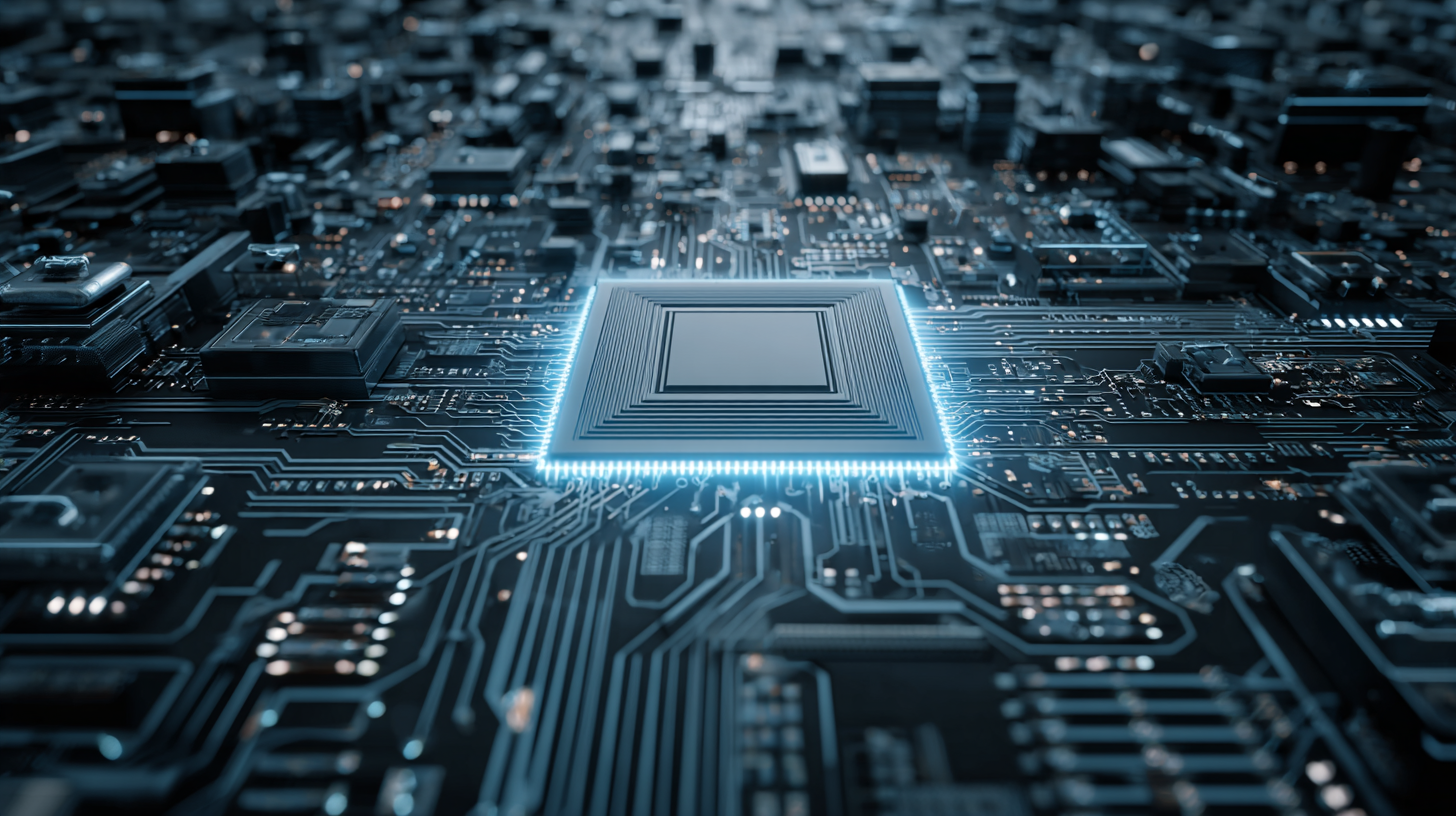
Innovative Approaches for Optimal Pcb Board Fabrication Success
The landscape of PCB board fabrication is rapidly evolving, driven by innovations and a global demand for high-quality electronics. According to a report by MarketsandMarkets, the global PCB market size is expected to reach USD 76.96 billion by 2024, growing at a CAGR of 3.7% from 2019. This growth underscores the importance of optimizing fabrication processes to enhance efficiency and reliability. As companies like those in China represent the forefront of intelligent manufacturing, dubbed "中国智造," they are not only fulfilling domestic needs but exporting quality products worldwide. Adopting innovative approaches in PCB board fabrication is essential to remain competitive and meet the unique demands of various industries, leveraging advances in technology to guarantee quality and performance. In this blog, we will explore these innovative strategies that are crucial for achieving success in the PCB board fabrication landscape.
Key Factors to Consider for Effective PCB Board Design
When it comes to effective PCB board design, several key factors play a crucial role in ensuring successful fabrication. First and foremost, understanding the electrical requirements of the circuit is essential. Designers must consider factors such as the voltage levels, current paths, and potential interference that could arise in complex systems. This knowledge guides the layout, enabling optimized trace widths and clearances that can withstand operational stresses while minimizing electromagnetic interference.
Another critical aspect revolves around material selection. The choice of substrate, copper thickness, and solder mask has a direct impact on the performance and durability of the PCB. High-frequency applications may require specific materials like FR-4 or Rogers to maintain signal integrity, while thermal management demands attention to factors like copper pour and thermal vias. Additionally, incorporating design for manufacturability (DFM) practices early on can help identify potential issues before they become costly errors during production. These considerations not only streamline the fabrication process but ultimately lead to a more reliable and robust end product.
Innovative Approaches for Optimal PCB Board Fabrication Success - Key Factors to Consider for Effective PCB Board Design
| Factor |
Description |
Impact on Design |
Recommended Practices |
| Material Selection |
Choosing the right substrate materials for durability and conductivity. |
High impact on signal integrity and longevity. |
Use of FR-4 or Polyimide materials based on application needs. |
| Layer Count |
Determining the number of layers required for complex circuit designs. |
Affects cost, size, and reliability of the PCB. |
Aim for minimal layers without sacrificing performance. Simplicity is key. |
| Trace Width |
Calculating appropriate trace width to carry the required current without overheating. |
Critical for preventing failure due to overheating. |
Use design calculators to determine optimal trace widths. |
| Ground Planes |
Utilizing continuous ground planes to reduce electromagnetic interference. |
Enhances signal integrity and stability. |
Incorporate ground planes in multilayer designs. |
| Design Software |
Selection of appropriate PCB design software for layout and simulation. |
Influences the efficiency and accuracy of the design process. |
Choose software with robust simulation capabilities. |
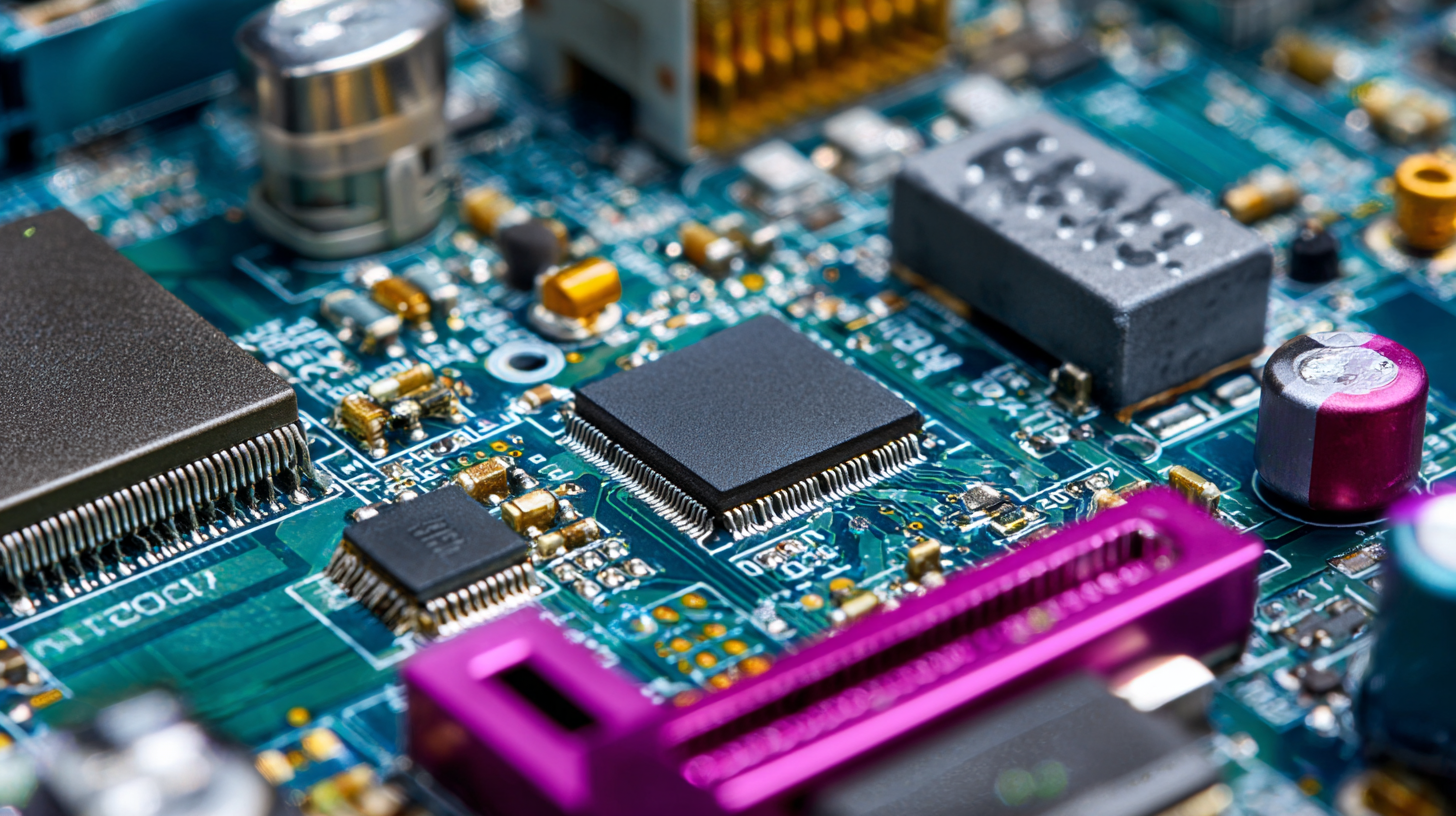
Advanced Materials and Their Impact on PCB Performance
The landscape of PCB (Printed Circuit Board) fabrication is continuously evolving, particularly with the introduction of advanced materials that enhance performance and reliability. According to a report by IPC, the global market for advanced PCB materials is projected to reach $3.4 billion by 2025, driven by the increasing demand for high-frequency applications and miniaturization in electronics. Materials such as high-density interconnect (HDI) laminates and flexible substrates offer superior thermal management and electrical performance, crucial for modern applications in telecommunications, automotive, and healthcare sectors.
One notable advancement is the use of organic substrate materials that exhibit lower dielectric loss, allowing for faster signal transmission and improved energy efficiency. Research indicates that PCBs utilizing these advanced materials can achieve a reduction in signal attenuation by up to 30%, making them highly desirable for 5G technologies and other cutting-edge applications. Furthermore, materials like polyimide are becoming prevalent due to their high thermal stability and excellent mechanical properties, enabling PCBs to perform reliably under extreme conditions. As manufacturers embrace these innovative materials, we can anticipate a significant enhancement in overall PCB performance, paving the way for future technological advancements.
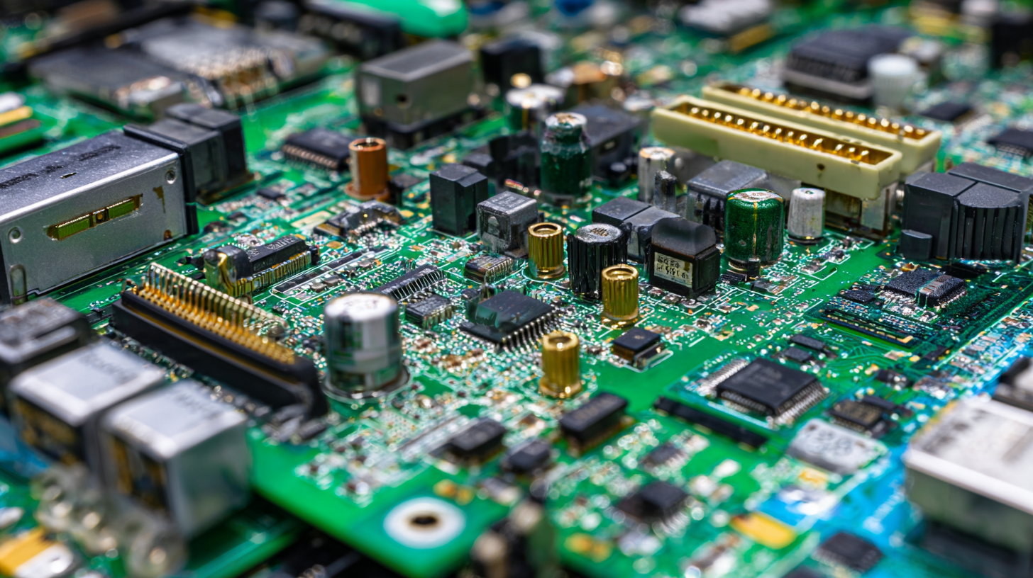
Streamlining the PCB Fabrication Process for Enhanced Efficiency
The PCB fabrication process is an intricate journey that can significantly impact the efficiency and quality of the final product. Recent industry reports indicate that optimizing this process can enhance productivity by as much as 30%. To achieve this, manufacturers are increasingly relying on advanced automation technologies, such as robotic arms and AI-driven monitoring systems, which streamline production and minimize human error. Implementing these technologies not only reduces lead times but also improves consistency in production runs.
Tips for Streamlining PCB Fabrication:
- Invest in automated inspection systems to identify defects early in the production cycle. This can cut down rework costs by nearly 20%.
- Utilize software tools for design-to-manufacturing feedback loops, allowing for real-time adjustments in the fabricating process. Reports suggest that this can enhance collaboration and reduce time-to-market by 15%.
- Adopt flexible manufacturing systems that can quickly adjust to changes in design specifications, thereby accommodating smaller batch sizes without impacting overall efficiency.
Continually evaluating and refining the PCB fabrication process is essential for staying competitive in today's fast-paced electronics market. By embracing innovative methods, manufacturers can lead the way in achieving operational excellence.
Innovative Technologies Shaping the Future of PCB Manufacturing
The rapid advancement of technologies is significantly shaping the future of PCB manufacturing, ushering in a new era where traditional methods are being transformed by innovative approaches. According to a report by IPC, the global PCB market is expected to reach $100 billion by 2026, driven by the increasing demand from various sectors including automotive, healthcare, and consumer electronics. This trend highlights the urgent need for manufacturers to adopt cutting-edge technologies that improve efficiency and reduce production costs.
One of the most promising technologies is additive manufacturing, or 3D printing, which enables the production of complex circuit designs that are not possible with conventional techniques. A study from Nanyang Technological University revealed that 3D printing can reduce PCB prototyping times by up to 90%, allowing for faster time-to-market for new products. Additionally, sustainable practices like the implementation of Eco-Friendly materials and waste recycling processes are becoming essential, as highlighted in the 2021 Global Electronics Industry report, which noted that 60% of consumers prefer brands that prioritize environmental responsibility. Overall, these innovative technologies not only enhance production efficiency but also align with the growing demand for sustainability in the electronics industry.
Quality Control Measures to Ensure PCB Reliability and Longevity
Quality control is a critical aspect of printed circuit board (PCB) fabrication that directly impacts the reliability and longevity of the final product. Implementing stringent quality control measures ensures that every stage of the PCB manufacturing process meets established standards. From the initial inspection of raw materials to the final testing of finished boards, maintaining high-quality benchmarks can prevent costly failures in the field. Advanced techniques such as automated optical inspection (AOI) and X-ray imaging can detect defects that might go unnoticed with the naked eye, ensuring that only the most reliable products are delivered to customers.
Incorporating robust testing protocols is also essential for verifying the performance and durability of PCBs. Techniques such as thermal cycling tests and vibration testing simulate real-world conditions that the boards might encounter, helping to identify potential weaknesses before they can cause problems. Additionally, integrating feedback loops and real-time monitoring systems during fabrication can help to quickly address any anomalies, adapting processes on the fly to enhance overall product quality. By committing to a proactive quality control strategy, manufacturers can not only increase customer satisfaction but also establish a reputation for reliability in a competitive market.
Quality Control Measures in PCB Fabrication
This chart illustrates the effectiveness of various quality control measures implemented in PCB fabrication across different metrics such as defect rates, testing success rates, and overall reliability ratings.